- 您现在的位置:买卖IC网 > Sheet目录237 > NSB13ANT3G (ON Semiconductor)TVS ZENER 600W 13V SMB
�� �
�
�NSB13ANT3G�
�APPLICATION� NOTES�
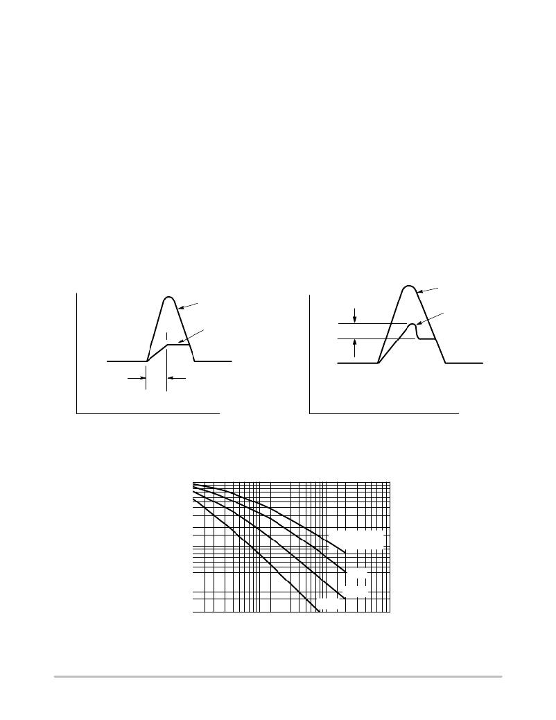
�RESPONSE� TIME�
�In� most� applications,� the� transient� suppressor� device� is�
�placed� in� parallel� with� the� equipment� or� component� to� be�
�protected.� In� this� situation,� there� is� a� time� delay� associated�
�with� the� capacitance� of� the� device� and� an� overshoot�
�condition� associated� with� the� inductance� of� the� device� and�
�the� inductance� of� the� connection� method.� The� capacitive�
�effect� is� of� minor� importance� in� the� parallel� protection�
�scheme� because� it� only� produces� a� time� delay� in� the�
�transition� from� the� operating� voltage� to� the� clamp� voltage� as�
�shown� in� Figure� 3.�
�The� inductive� effects� in� the� device� are� due� to� actual�
�turn‐on� time� (time� required� for� the� device� to� go� from� zero�
�current� to� full� current)� and� lead� inductance.� This� inductive�
�effect� produces� an� overshoot� in� the� voltage� across� the�
�equipment� or� component� being� protected� as� shown� in�
�Figure� 4.� Minimizing� this� overshoot� is� very� important� in� the�
�application,� since� the� main� purpose� for� adding� a� transient�
�suppressor� is� to� clamp� voltage� spikes.� The� SMB� series� have�
�a� very� good� response� time,� typically� <� 1� ns� and� negligible�
�inductance.� However,� external� inductive� effects� could�
�produce� unacceptable� overshoot.� Proper� circuit� layout,�
�minimum� lead� lengths� and� placing� the� suppressor� device� as�
�close� as� possible� to� the� equipment� or� components� to� be�
�protected� will� minimize� this� overshoot.�
�Some� input� impedance� represented� by� Z� in� is� essential� to�
�prevent� overstress� of� the� protection� device.� This� impedance�
�should� be� as� high� as� possible,� without� restricting� the� circuit�
�operation.�
�DUTY� CYCLE� DERATING�
�If� the� duty� cycle� increases,� the� peak� power� must� be�
�reduced� as� indicated� by� the� curves� of� Figure� 5.� Average�
�power� must� be� derated� as� the� lead� or� ambient� temperature�
�rises� above� 25� °� C.� The� average� power� derating� curve�
�normally� given� on� data� sheets� may� be� normalized� and� used�
�for� this� purpose.�
�V�
�V� in� (TRANSIENT)�
�V�
�OVERSHOOT� DUE� TO�
�INDUCTIVE� EFFECTS�
�V� in� (TRANSIENT)�
�V� L�
�V� L�
�V� in�
�t� d�
�t� D� =� TIME� DELAY� DUE� TO� CAPACITIVE� EFFECT�
�Figure� 3.�
�t�
�Figure� 4.�
�t�
�1�
�0.7�
�0.5�
�0.3�
�0.2�
�PULSE� WIDTH�
�0.1�
�0.07�
�0.05�
�0.03�
�0.02�
�10� m� s�
�10� ms�
�1� ms�
�100� m� s�
�0.01�
�0.1� 0.2�
�0.5�
�1�
�2� 5� 10�
�20�
�50� 100�
�D,� DUTY� CYCLE� (%)�
�Figure� 5.� Typical� Derating� Factor� for� Duty� Cycle�
�http://onsemi.com�
�4�
�发布紧急采购,3分钟左右您将得到回复。
相关PDF资料
NSQA12VAW5T2G
TVS QUAD ARRAY LO CAP ESD SOT323
NUP1105LT3G
IC BUS PROTECTOR CAN/LIN SOT-23
NUP1301ML3T1G
IC DIODE ARRAY LOCAP ESD SOT-23
NUP1301U,115
IC DIODE ARRAY ESD SC-70
NUP2114UCMR6T1G
TVS ARRAY ESD 6-TSOP
NUP2201MR6T1
IC TVS DIODE ARRAY HS LINE 6TSOP
NUP2202W1T2G
IC DIODE/TVS ARRAY HS SOT-363
NUP2301MW6T1
IC TVS DIODE ARRAY 2LINE SC88
相关代理商/技术参数
NSB13ANT3H
制造商:ON Semiconductor 功能描述:
NSB1706DMW5T1
功能描述:开关晶体管 - 偏压电阻器 100mA 50V BRT NPN RoHS:否 制造商:ON Semiconductor 配置: 晶体管极性:NPN/PNP 典型输入电阻器: 典型电阻器比率: 安装风格:SMD/SMT 封装 / 箱体: 直流集电极/Base Gain hfe Min:200 mA 最大工作频率: 集电极—发射极最大电压 VCEO:50 V 集电极连续电流:150 mA 峰值直流集电极电流: 功率耗散:200 mW 最大工作温度: 封装:Reel
NSB1706DMW5T1/D
制造商:未知厂家 制造商全称:未知厂家 功能描述:Dual Bias Resistor Transistor
NSB1706DMW5T1G
功能描述:开关晶体管 - 偏压电阻器 100mA 50V BRT NPN RoHS:否 制造商:ON Semiconductor 配置: 晶体管极性:NPN/PNP 典型输入电阻器: 典型电阻器比率: 安装风格:SMD/SMT 封装 / 箱体: 直流集电极/Base Gain hfe Min:200 mA 最大工作频率: 集电极—发射极最大电压 VCEO:50 V 集电极连续电流:150 mA 峰值直流集电极电流: 功率耗散:200 mW 最大工作温度: 封装:Reel
NSB1706DMW5T1G_09
制造商:ONSEMI 制造商全称:ON Semiconductor 功能描述:Dual Bias Resistor Transistor
NSB1A-8/4
功能描述:扬声器连接器 STAGE BX 8 IN F/SND 4 OUT MALE/RETURN
RoHS:否 制造商:Neutrik 标准:Speakon, HPC 型式:Male 位置/触点数量:2 端接类型: 安装风格:PCB 方向:Vertical 触点电镀: 颜色: 触点材料: 电压额定值: 电流额定值:
NSB1B-8/0
功能描述:扬声器连接器 STAGE BX 8 IN F/SND
RoHS:否 制造商:Neutrik 标准:Speakon, HPC 型式:Male 位置/触点数量:2 端接类型: 安装风格:PCB 方向:Vertical 触点电镀: 颜色: 触点材料: 电压额定值: 电流额定值:
NSB1C-8/0
功能描述:扬声器连接器 STAGE BX 8 IN F/SND
RoHS:否 制造商:Neutrik 标准:Speakon, HPC 型式:Male 位置/触点数量:2 端接类型: 安装风格:PCB 方向:Vertical 触点电镀: 颜色: 触点材料: 电压额定值: 电流额定值: